- 您现在的位置:买卖IC网 > Sheet目录350 > PG-FP4-E (Renesas Electronics America)PROGRAMMER FLASH MEMORY UNIV
CHAPTER 8 NOTES ON TARGET SYSTEMS
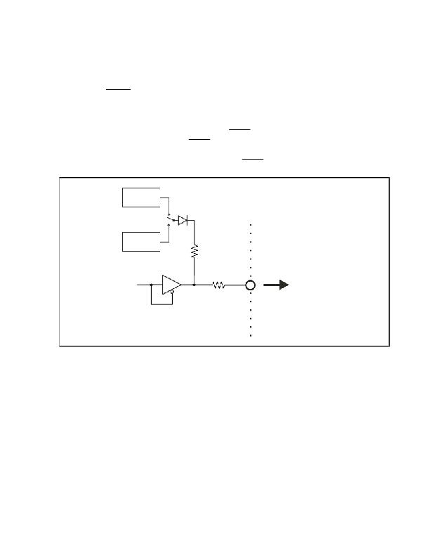
The following show examples of the interface circuits of UART (asynchronous communication port) and SIO (3-wire
clocked communication port).
Refer to the above design proposal for the pin processing of the device to be used.
? Using two-power-supply flash memory microcontroller
Figure 8-1. UART Interface Circuit Example
V CC
V CC
IC
C
SI 5
7
CLK 9
2
4
6
8
10
Connector
1
RESET GND 3
V DD
V PP SO
H/S SCK
VDE
1 k ?
TxD
RxD
X1
X2
Y
C
FAP-1008#2
V CC
V PP
RESET
R
V CC
1 k ?
V DD
V SS
R
JUMPER
User reset circuit
Microcontroller
Caution1.
2.
3.
4.
Insert neither capacitors nor resistors into the V PP line unless otherwise stated. When pull-
down resistors are inserted into the V PP line, the resistor value must be 470 ? or higher.
The PG-FP4 generally performs normally without pin processing.
If the pins of the PG-FP4's output signals (SO/TxD) are processed, pull up (or pull down) with a
resistor value in compliance with the specifications (V IH , V IL ) of the target device, referring to
CHAPTER 9 TARGET SYSTEM INTERFACE CIRCUITS.
If the pins of the PG-FP4's input signals (SI/RxD, RESET) are processed, pull up (or pull down)
with a resistor value in compliance with the specifications (I OH , I OL ) of the target device,
referring to CHAPTER 9 TARGET SYSTEM INTERFACE CIRCUITS.
User ’s Manual U15260EJ4V0UM
97
发布紧急采购,3分钟左右您将得到回复。
相关PDF资料
PG15S-D20-HHB9
MOTOR GEARED STEPPER 15MM 15V BI
PG164120
PROGRAMMER MCU PICKIT 2
PG20L-D20-HHC0
MOTOR GEARED STEPPER 20MM 10V BI
PG25L-D24-HHC1
MOTOR GEARED STEPPER 25MM 24V BI
PG35S-D48-HHC2
MOTOR GEARED STEPPER 35MM 24V BI
PIC12F683 DEVELOPMENT KIT
KIT DEV EMBEDDED C
PIC18F4520 DEVELOPMENT KIT
KIT DEV EMBEDDED C
PIC18F67J10 DEVELOPMENT KIT
KIT DEV EMBEDDED C
相关代理商/技术参数
PG-FP5
制造商:Renesas Electronics Corporation 功能描述:MCU,Programmer,NEC Flash MCU
PG-FP5-AS
制造商:Renesas Electronics Corporation 功能描述:MICROCOMPUTER FLASH MEMORY PROGRAMMER 制造商:Renesas Electronics Corporation 功能描述:PROGRAMMER FLASH RL78 V850 7
PG-FP5-EA
功能描述:PROGRAMMER FLASH MEMORY UNIV RoHS:是 类别:编程器,开发系统 >> 内电路编程器、仿真器以及调试器 系列:* 产品变化通告:Development Systems Discontinuation 19/Jul/2010 标准包装:1 系列:* 类型:* 适用于相关产品:* 所含物品:*
PGFP-A11
功能描述:PLUG GFCI 120VAC 15/20A AUTORST RoHS:是 类别:过电压,电流,温度装置 >> 接地故障电路断路器 (GFCI) 系列:PGFP 标准包装:1 系列:PGFI 类型:带 6 英尺引线的直列接头 技术规格:120V 其它名称:723-1041
PGFP-A110KYST2
功能描述:CORD GFCI 120VAC 2' YEL SNG TAP RoHS:是 类别:过电压,电流,温度装置 >> 接地故障电路断路器 (GFCI) 系列:PGFP 标准包装:1 系列:PGFI 类型:带 6 英尺引线的直列接头 技术规格:120V 其它名称:723-1041
PGFP-A110KY-ST2
制造商:Airpax 功能描述:
PGFP-A110KYST25
功能描述:CORD GFCI 120VAC 25' YEL SNG RoHS:是 类别:过电压,电流,温度装置 >> 接地故障电路断路器 (GFCI) 系列:PGFP 标准包装:1 系列:PGFI 类型:带 6 英尺引线的直列接头 技术规格:120V 其它名称:723-1041
PGFP-A110KYTT2
功能描述:CORD GFCI 120VAC 2' YEL TRITAP RoHS:是 类别:过电压,电流,温度装置 >> 接地故障电路断路器 (GFCI) 系列:PGFP 标准包装:1 系列:PGFI 类型:带 6 英尺引线的直列接头 技术规格:120V 其它名称:723-1041
